optical inspection (MOI/AOI/SPI)
It is impossible to imagine our world without electronics: they connect us and simplify our lives. That's why we want to excel. Our innovations do just that. We leave nothing to chance: from material and functional tests to final testing of our products and services. But we go even further and supplement our quality management with additional test systems and our own quality standards.
Comprehensive operational and machine data acquisition and the traceability system we use enable the traceability of all produced assemblies and components, as well as the processes used for this. In addition, an ERP system maps all business processes and guarantees the effective use of all resources throughout the company. This ensures an efficient operational value creation process and helps to optimize business and operational processes.
The entire company is certified in accordance with the DIN EN ISO 9001:2015 quality standard. In addition, production is regularly monitored in accordance with the ESD protection concept DIN EN 61340, which rules out any disruption to the production process caused by electrostatic charges.
The top priority of our company philosophy is the consistently high quality and safety of our products. For this reason, type and series tests are a very important part of our production process in all development and manufacturing processes. We are aware of our great responsibility towards our customers. This is why our demand for the consistently high quality and safety of our products can only be the highest. Type and series tests are therefore a very important part of our production process in all development and manufacturing processes. Depending on the area of application, the following inspection and test systems are used: manual optical inspection (MOI), automatic optical inspection (AOI), automatic X-ray inspection (AXI), function test (FCT), flying probe test (FPT) and high voltage test (HV Test).
Everything from a single source: Our customers benefit above all from the fact that we provide the entire service, from development and production to the testing of all products - whether as an individual service or as a complete package - in-house. Constant monitoring of test equipment prevents incorrect decisions and incorrectly tested assemblies. An individual test concept is tailored to the requirements and ideas of our customers. All measurements and test results are documented in a test report, as is every work step, thus ensuring permanent traceability.

We inspect and test for optimum results. Manual optical inspection (MOI) is used for prototypes and small series for which automatic optical inspection is too time-consuming. Defect patterns can be recognized and documented very well. An MOI solution is particularly suitable for the inspection of pilot series and prototypes or when process parameters are changed.
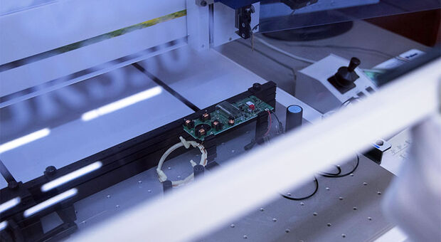
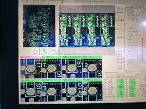
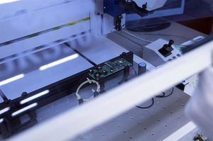
We leave nothing to chance. Automatic optical inspection (AOI) is an optical structure test for printed circuit boards that detects mechanically defective components, press-fit errors, assembly errors and soldering errors.
After the reflow (SMD) and wave soldering (THT) processes, the assemblies are subjected to an automatic optical inspection. As these process steps are very complex, a variety of possible causes can lead to production errors and failure of the electronic assembly. For this reason, the assemblies are also optically inspected. With our stand-alone solution of the AOI system, the following production steps are subjected to an optical inspection:

SPI stands for "Solder Paste Inspection". The purpose of SPI is to detect defects by analyzing the condition of solder paste deposits that have been applied by a screen printer for PCB assembly. The results of the inspection are used to adjust the parameters of the screen printer so that the printing process can be optimized to avoid possible errors.
Solder paste inspection is an advanced method for improving quality while reducing operating costs. The costs for possible rework in the initial phase of the production process are significantly lower than in later stages.
Solder paste inspection is performed in-line in our 4 SMT lines. We use the Omron CKD VP5200 machines.

Our commitment to optimum functionality. During the functional test (FCT), the product is tested for its functional requirements. For customer-specific products, we offer our own solutions or use supporting systems from partners.
A functional test is often carried out on prefabricated components before final assembly. Simultaneous programming of processors is possible (in-system programming). The function test simulates/emulates the real environment and thus forces switching operations that can otherwise only be checked in the installed state. Voltages, currents and other measured variables are set and switching sequences are executed as they would be in reality.
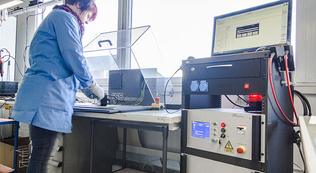
We hold the voltage. A high-voltage test is used to ensure the insulation strength of electronic components in the low-voltage range (protection classes I and II). The insulation of the current-carrying conductors and the safety distance to the housing are tested.
In contrast to insulation measurement, a high-voltage test is a dielectric strength test that checks the prescribed insulation distances. As a rule, a high-voltage test is carried out from the short-circuited main circuit (phase and neutral conductor) to the protective conductor.
The test time and test voltage are defined differently depending on the standard and protection class and can be between 1000V AC and 6000V DC. No flashover or breakdown may occur during the test.
We put our electronic products to the test for you. The flying probe test (FPT) is an electrical test procedure for printed circuit boards in which test points are probed sequentially. It is the method of choice for missing test pads or assemblies that are difficult to contact.
This test method can be used to detect most faults such as press-fit errors, defective electrical components, assembly errors, soldering errors and short circuits.


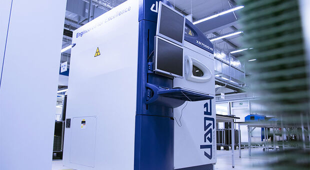
Automatic X-ray inspection (AXI) is used to check assembled printed circuit boards. Similar to automatic optical inspection (AOI), X-rays are used instead of light. X-ray inspection is a non-destructive way of analyzing printed circuit boards and other electronic assemblies in the electronics industry, particularly in the assembly of printed circuit boards. It is frequently used in quality control during production and development.
We use a system from the manufacturer Nordson DAGE XD7500VR as a stand-alone solution. The working and scanning surface for testing printed circuit boards has an area of 51.5 cm in depth and 45 cm in width.